 Intelligent Manufacturing Process Area in Processing for Manufacturing
Division of Materials and Manufacturing Science
Graduate School of Engineering, Osaka University
Intelligent Manufacturing Process Area in Processing for Manufacturing
Division of Materials and Manufacturing Science
Graduate School of Engineering, Osaka UniversityResearch
Nanojoining and Microjoining
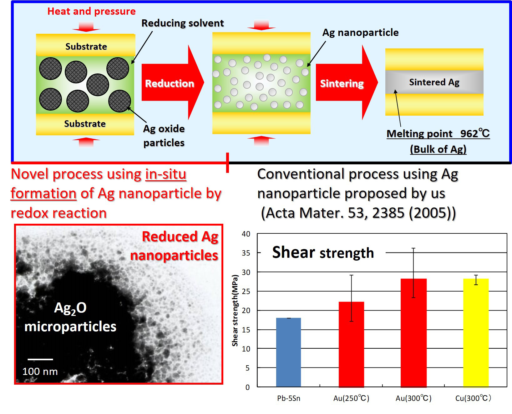
We succeeded in developing the world's first Ag nanoparticle joining process (Ide, Hirose, Acta Materialia 2003), which is the worldwide standard process with high temperature reliablity in electronics field. At present, we investigate the applied process based on the fundamental knowledge, such as reduction behavior, sintering behavior and interfacial reaction, in addition to the development of next-generation joining process for electronics.
- Low-temperature joining process using nanoparticles derived from the decomposition of metal oxide
- Sinter joining using the reduction of silver oxide enables the joining of various metals We succeeded in achieving the joining for various metals using Ag2O microparticles or copper oxide (CuO and Cu2O) particles. In addition, we have applied such reduction-induced nanosintering to the other joining process such as micro resistance spot welding and SHS joining. Paper:J. Electron. Mater. 47, 2193 (2018), Mater. Trans. 56, 1030 (2015), Mater. Trans. 56, 866 (2013), Mater. Charact. 98, 186 (2014), J. Electron. Mater. 42, 502 (2013), J. Electron. Mater. 41, 2573 (2012), Mater. Trans. 50, 226 (2009).
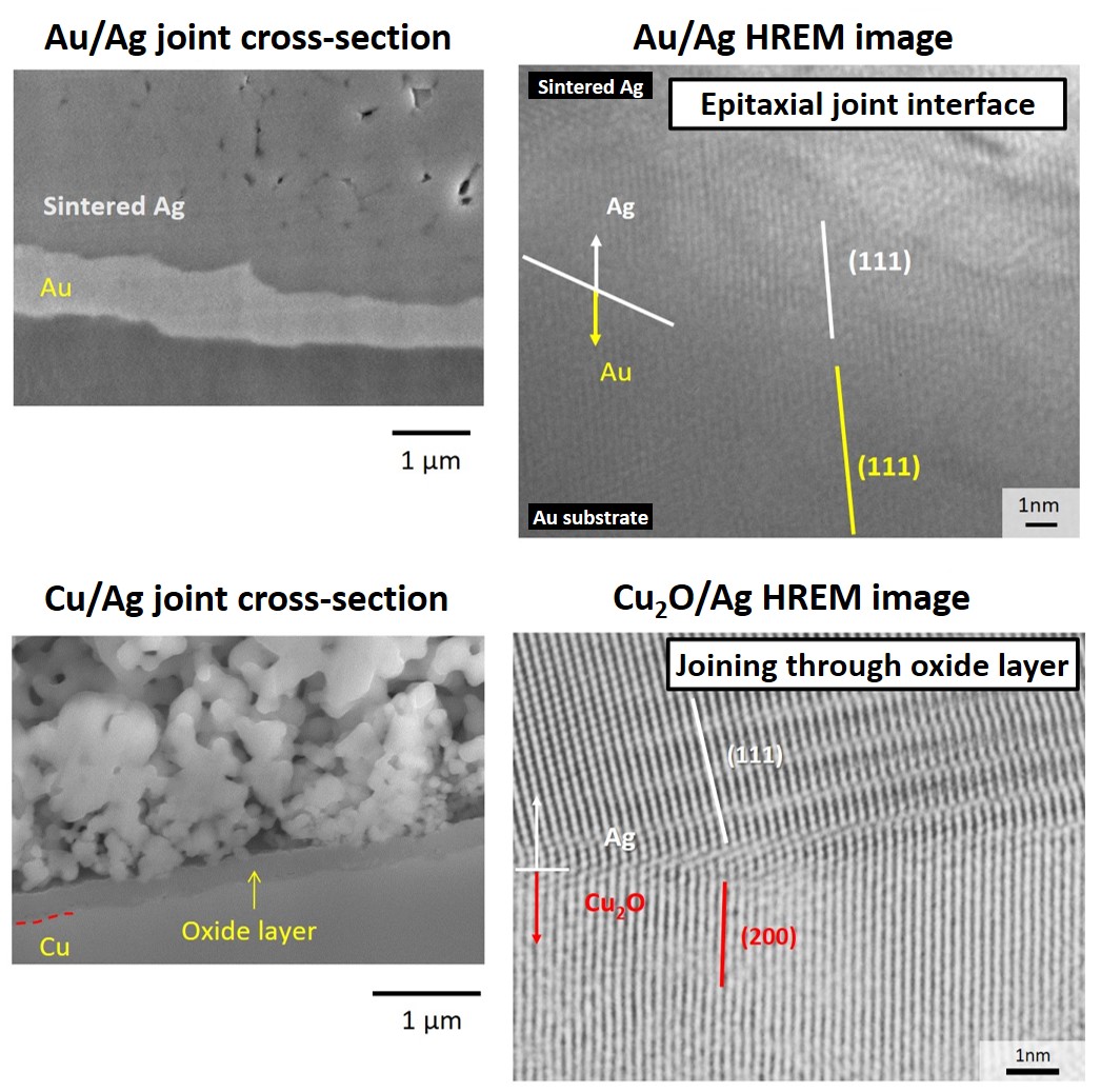
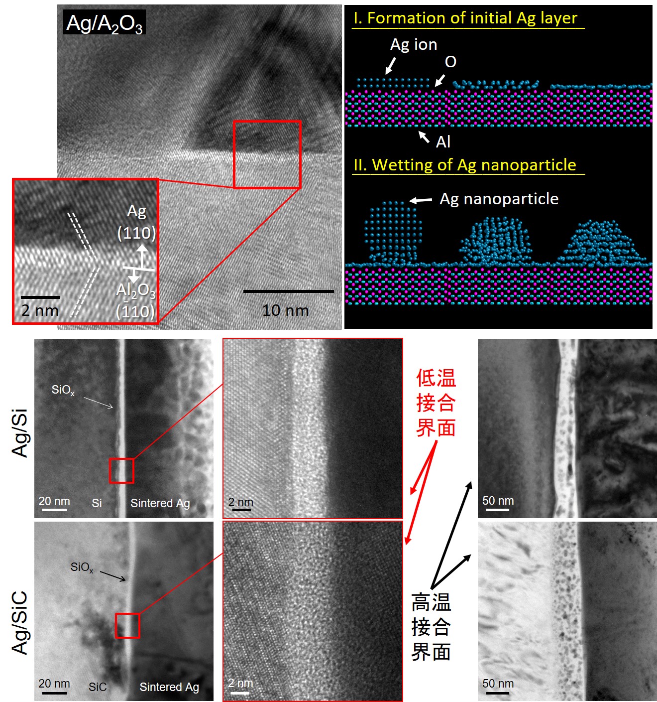
- Metallization-free direct sinter joining for metal/non-metal Our joining process ensures the direct joining between metal and non-metal such as silicon, sapphire, aluminum nitride, quartz, silicon carbide, and silicon nitride, which have difficulty in the conventional sinter joining. This is because the atomic-nano scale interfacial reaction during the decomposition facilitates the interfacial bonding. Paper:Scientific Reports 8, 10472 (2018), J. Electron. Mater. 47, 5780 (2018), J. Electron. Mater. 47, 2193 (2018). Materials Science & Engineering A 702, 398 (2017), J. Electron. Mater. 46, 6488 (2017), Journal of Smart Processing 8, 177 (2019), Journal of Smart Processing 6, 132 (2017), Journal of Materials Science: Materials in Electronics (accepted).
- Development of novel microjoining process We proposed novel microjoining process based on our unique idea for the next-generation power modules. We obtained high-reliable joints through following process. Paper:Materials & Design 160, 475 (2018), Applied Science 9, 157 (2019), Journal of Electric Materials 48, 3699 (2019), Applied Sciences 9, 3476 (2019), IEEE Transaction on Components, Packaging and Manufacturing Technology, 9, 2111(2019), J. Electron. Mater. 46, 4326 (2017).
 Novel solder-metallic mesh composite design.
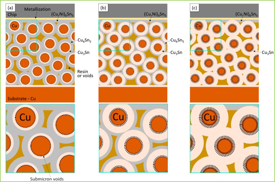 Transient Liquid-Phase Sintered Cu-Sn Skeleton Microstructure.